
The Substrate Wars: A Reality Check + Investor’s Playbook for the AI Packaging Revolution

Everyone is watching the chips; almost no one is watching what carries them. In the shadow of the GPU and HBM boom, a quiet crisis is brewing at the foundation of the semiconductor stack. As process nodes shrink below 2nm and packaging shifts to complex 2.5D/3D Chiplet architectures, the humble organic substrate has emerged as the single greatest bottleneck for AI performance. We are witnessing a bifurcation in the material supply chain:
The Glass Core Faction (The Revolutionaries): Betting that Moore’s Law can only be saved by abandoning organic chemistry for silicate physics.
The Advanced Composite Alliance (The Incumbents): Betting that chemical engineering can “hack” plastics to behave like glass.
This article analyzes this showdown in depth and provides a severe reality check specifically regarding commercialization timelines and investment risks.
The Physics of the Business: The Limits of the Plastic Era
Before discussing who wins and who loses, it is essential to understand that this war is fundamentally a battle against the laws of physics. The explosive growth in computing power of AI chips (such as NVIDIA Blackwell or Google TPU) has hit two physical walls:
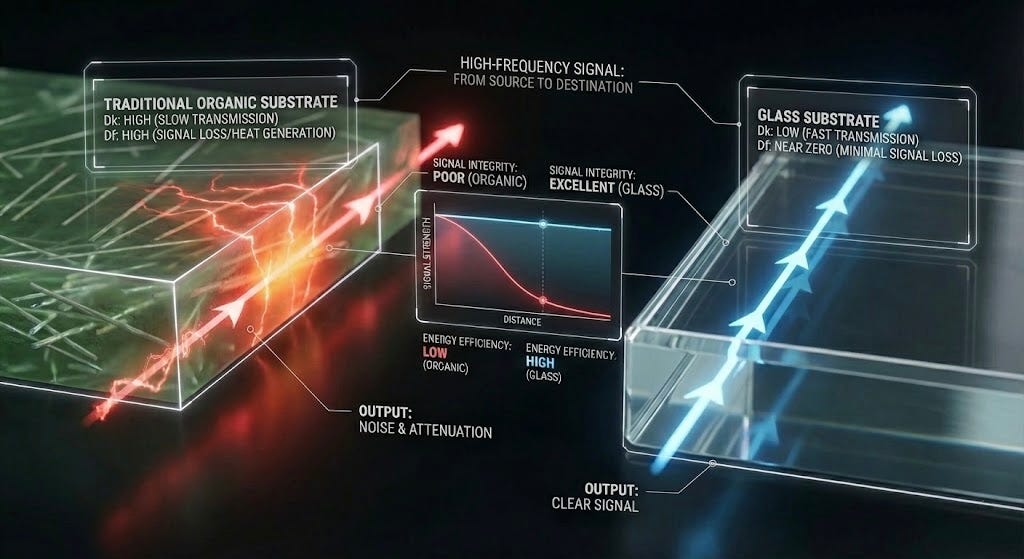
1. Signal Integrity & Skin Effect
When data transmission speeds exceed 112 Gbps (and move toward 224 Gbps PAM4), electric current no longer flows through the center of the conductor but is instead squeezed onto the conductor’s surface. This is known as the “Skin Effect.”
The Physics: The signal transmission speed depends on the speed of light divided by the square root of the Dielectric Constant (Dk).
The Problem: Traditional organic substrates (composed of resin and standard glass fibers) have a Dk value that is too high and a Df (dissipation/loss factor) that is too large. This means high-frequency signals are “eaten up” by the substrate during transmission (converted into heat), causing the signal to arrive at the other end as mere noise.
The Challenge: We need a material with a low enough Dk (fast transmission) and a virtually zero Df (no signal loss).
The Glass Advantage: Glass’s Df is almost zero, which is its greatest physical advantage.
Layman Language: Imagine the data signal is a sports car and the substrate is the road. Traditional organic substrates are like a “muddy gravel road” (high friction/high loss)—the car cannot drive fast and the engine overheats. Glass substrates are like a “Maglev track” (zero friction)—the signal can travel at maximum speed without losing energy.
2. Thermomechanical Stress & CTE Mismatch
Physical Background: The Coefficient of Thermal Expansion (CTE) of the silicon chip is approximately 2.6 ppm/°C. The CTE of a traditional organic substrate is about 12 to 17 ppm/°C.
Disaster Scenario: When the package is heated to 250°C in the reflow oven, the substrate expands much faster than the chip. Upon cooling, the substrate shrinks faster than the chip.
The Result: This “pulling and tugging” creates enormous Shear Stress, causing thousands of tiny solder bumps to fracture, or the substrate itself to warp like a potato chip (Warpage).
The Glass Advantage: The CTE of glass can be precisely tuned to match that of silicon, fundamentally eliminating this “thermal fighting.”
The Glass Process Revolution — An Engineering “Moonshot”
If glass is so good, why are we only discussing it in 2025? Because glass defies traditional manufacturing logic: it is too brittle. Here is how leading manufacturers (such as Absolics and the Intel supply chain) are solving mass production challenges through “Three Major Physical Techniques”:
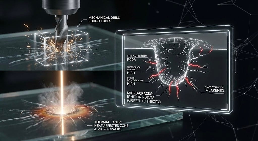
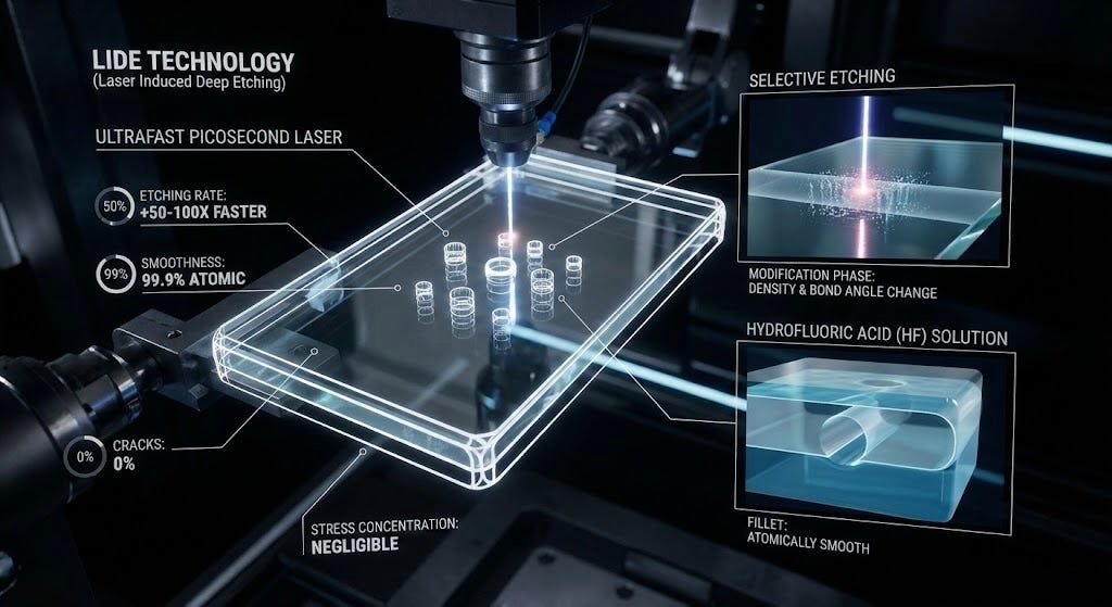
The Drilling Revolution: LIDE Technology (Laser Induced Deep Etching)
The Challenge: How do we drill millions of holes in glass without shattering it?
Traditional Error: Using mechanical drills or high-power thermal lasers. These methods create Micro-cracks on the hole walls. According to Griffith’s Theory, these cracks are ignition points for stress concentration.
Modern Solution (LIDE):
Modification: An ultrafast picosecond laser is fired into the glass. It does not remove material but changes the local chemical bond angles and density inside the glass.
Selective Etching: The glass is immersed in a Hydrofluoric Acid (HF) solution.
Chemical Magic: The etching rate in the modified areas is 50 to 100 times faster than in the unmodified areas. The acid instantly etches a perfect channel.
Result: The hole walls are atomically smooth with rounded edges (Fillet). No cracks equal no stress concentration, making the glass stronger.
The Interface Revolution: Ti/Cu Chemical Bonding
The Challenge: How do we “grow” copper wiring on a super-smooth glass surface?
Physical Problem: Glass is too smooth; there is no roughness for the copper to mechanically “grip” onto.
Chemical Solution:
Vacuum Sputtering (PVD): In a high-vacuum environment, titanium atoms are bombarded onto the glass surface.
Covalent Bond Formation: Titanium (Ti) is highly reactive and loves oxygen. It reacts with the silicon dioxide (SiO2) in the glass to form Ti-O-Si covalent bonds. This nanometer-thin titanium layer acts as the strongest possible “molecular glue.”
Plating: Copper is then built on top of this titanium layer.
Conclusion: We no longer rely on roughness but on chemical bonds. This solves the contradiction between adhesion and signal smoothness.
Stress Management: Polymer Stress Buffer Layer
The Challenge: How to prevent the copper’s thermal expansion from tearing the glass apart?
Solution: A layer of special photosensitive polymer (or PI) is coated between the glass and the metal layers.
Function: This material possesses Viscoelasticity. When the copper heats up and expands, the polymer layer stretches elastically, absorbing most of the shear stress and protecting the fragile glass underneath.
The Reality Gap: Why “Technically Possible” ≠ “Commercially Viable”
If the physics is solved (as shown above), why isn’t Nvidia using glass today?
This is the single most important concept for investors to grasp: Technology Readiness Level (TRL) is not Manufacturing Readiness Level (MRL).
The Lab vs. The Fab: In a lab, money is no object. You can spend $10,000 to make one perfect glass interposer using LIDE and PVD. The physics works.
The Economic Wall: In a commercial foundry, you must make millions of units at $500 each. The challenge shifts from “Can we do it?” to “Can we do it 10,000 times in a row without a single error?”
The Disconnect: We are currently in the dangerous gap where the science is ready, but the unit economics are broken. The manufacturing speed is too slow, and the defect rate is too high. This leads us directly to the financial leverage that controls the entire industry: Yield.
The Cruel Math of Yield — Why 50% Is Both Disaster and Hope
In semiconductor manufacturing, “Yield” is the financial leverage that determines life or death. Currently, the yield for glass substrates is hovering around 50%.
1. Why is 50% Yield a “Major Victory” in a Pilot Run?
Despite the high cost, reaching 50% at this stage is a critical inflection point for companies like Absolics and Intel:
Physics Problem vs. Engineering Problem: Moving from 0% to 10% is a “Science Problem” (meaning the path might be physically impossible). Moving from 10% to 50% means the underlying physical principles are “Proven Physics.”
Investment Signal: The climb from 50% to 90% is now just “Engineering Discipline” (cleaner cleanrooms, better automation, more precise inspection). The technological risk is gone; only execution risk remains. It is now a problem that can be solved with money.
2. Why is 50% Yield an Absolute Disaster in High Volume Manufacturing (HVM)?
In a real factory, a 50% yield means massive financial losses due to:
The Vampire Effect: This is lethal. The glass substrate is just the carrier; mounted on top of it are Nvidia H100s or Google TPUs (valued at $30,000+). If the substrate has a hidden defect, it kills the expensive chip attached to it. You don’t just lose the $500 glass; you lose the entire $30,500 assembly.
Analogy: This is like putting a cheap $500 tire on a $3 million Ferrari. If the tire blows out and wrecks the car, your loss isn’t just the tire—it’s the whole Ferrari. Customers will not accept glass risks until yields exceed 99% for this exact reason.
Halved Capacity: Fixed factory depreciation costs (billions of dollars) are spread over only half the output. Unit costs double instantly, swallowing all gross margin.
The Advanced Composite Alliance (The Incumbents)
Faced with the threat from glass, the Japanese material science industry has formed a powerful defensive line. They reject the label of “fragile plastic.” Their argument is simple: “If we engineer composites to perform like glass, you don’t need real glass.”
Nittobo’s Strategic Weapon: Low-CTE “T-Glass” Reinforcement
Material Science: Traditional glass fiber (E-Glass) expands at about 5-6 ppm. Nittobo adjusted the formula (increasing aluminum oxide/boron oxide) to create T-Glass, lowering expansion to 3.0-3.2 ppm.
Strategy: When this special fiber is used as the “skeleton” of the substrate, it forcefully limits the expansion of the resin.
Result: Organic substrates using T-Glass can achieve an overall expansion of 7-9 ppm. While still higher than silicon (2.6 ppm), it is “good enough” for chips like the Nvidia H100, and costs only 1/3 of a glass substrate.
Resonac’s Armor: Ultra-High Filler Composites
Logic: If the resin is too soft, fill it with rocks.
Process: Resonac (formerly Showa Denko) uses nano-dispersion to mix spherical silicon dioxide (SiO2) powder into the resin, achieving a filler rate of 85%.
Result: Although called an “organic substrate,” 85% of it is essentially stone. Its rigidity is vastly improved, preventing warping.
The Hybrid Solution: Mitsui Kinzoku’s HRDP
Concept: A Carrier-based System.
Process: Use a glass piece as a temporary base to build ultra-fine circuits (2 microns). Once finished, use a laser to detach (debond) the base glass and throw it away.
Threat: This allows organic substrates to achieve glass-level precision without the fragility issues of the final product. This is the biggest transitional threat to pure glass.
The Contenders & Real Evidence – Breaking the “Paper Tiger” Myth
If you look at the yield challenges, it would be easy to conclude that glass substrates are impossible. However, despite the “yield wall” and the brutal physics involved, the industry has moved past the phase of PowerPoints and Science Fiction. We are now witnessing a tangible shift from R&D to HVM (High Volume Manufacturing).
The following players are not just experimenting; they are pouring concrete, installing billion-dollar equipment, and locking in government subsidies. They are betting their future that they can solve the 50% yield problem before they run out of cash.
SKC - Absolics (The Aggressor)
Role: The First Mover & US-Aligned Specialist
Status: Fastest progress globally; currently in the “Valley of Death” (scaling up).
The Evidence:
Factory: Their Phase 1 factory in Covington, Georgia, USA, is physically complete (a $600 million investment). This is not a plan; the building exists.
Subsidy Win: They were the first materials manufacturer to be proposed a direct $75 million subsidy from the US CHIPS Act. This is a massive signal that the US government views Absolics as a critical supply chain partner for Nvidia/AMD, rather than relying solely on Asian supply chains.
Partnerships: Deeply tied to the AMD ecosystem, specifically targeting the next generation of AI accelerators.
Core Technology & Strategy:
Absolics uses a proprietary material formulation developed by its parent company, SKC.
Focus: They are aggressively pushing Passive Component Integration. They are not just making a glass board; they are embedding capacitors (MLCCs) inside the glass to save space and improve power efficiency for AI chips.
Timeline: They are currently running qualification samples. Mass production is targeted for late 2025 to early 2026, making them the “canary in the coal mine”—if they succeed, the market explodes; if they fail, the industry delays.
Intel (The Architect)
Role: The Standard Setter & Long-Term R&D Leader
Status: The setter of technical specifications with the deepest IP portfolio.
The Evidence:
Investment: Announced a $1 billion investment dedicated solely to a glass substrate pilot line at their Chandler, Arizona campus.
History: Intel didn’t just start this because of the AI boom; they have been researching Through-Glass Vias (TGV) for over a decade.
Demonstration: In late 2023, they publicly showcased fully functional test vehicles (glass core wafers) that proved the mechanical reliability of their TGV technology.
Core Technology & Strategy:
TGV Density: Intel is focusing on density. They claim their glass technology can put 10 times more holes (vias) in the same area compared to organic packaging, allowing for massive data bandwidth.
The “Systems Foundry” Play: Intel isn’t just making this for their own chips; they want to offer glass packaging as a service to outside customers (like Microsoft or Amazon) through Intel Foundry Services (IFS).
Timeline: Conservative. Their official target is 2026-2030. Intel is realistic about the “Yield Wall” and is unwilling to ship until the process is as reliable as their traditional organic lines.
Samsung Electro-Mechanics / SEMCO (The Fast Follower)
Role: The Integration Master Status: Attempting to replicate their dominance in Memory and OLED by leveraging internal synergy.
The Evidence:
Organizational Pivot: In early 2024, Samsung CEO Kyay-Hyun Kyung elevated the glass substrate project to a top-tier priority, establishing a “Glass Substrate Promotion Team” that reports directly to leadership.
Execution: A pilot line has already been installed at their Sejong City factory in South Korea.
Core Technology & Strategy:
The “Total Package” Advantage: Samsung is unique because they own the entire chain: they make the memory (HBM), they make the chips (Foundry), and they make the capacitors (MLCC).
Tech Strategy: Their goal is to build a “Unified Glass System” where the glass substrate, the HBM memory stack, and the GPU are packaged together in one house. This reduces the risk of supply chain finger-pointing if something fails.
Timeline: Extremely aggressive. They are targeting prototype samples in 2025 and mass production in 2026, trying to close the gap with Intel by utilizing their massive manufacturing muscle.
The glass substrate war is not a monolith; it is a three-way race with distinct strategic flavors. While Absolics sprints for first-mover advantage, Intel plays the long game of ecosystem dominance, and Samsung leverages its unique vertical integration.
In-Depth Analysis & Investment Strategy – A Reality Check
The hype around Glass Substrates has hit a fever pitch, but mistaking physical superiority for investment-grade reality is a dangerous error. While retail capital chases ‘science projects,’ smart money understands that the revolution is effectively paused until one specific gatekeeper gives the order. This sector is currently a minefield of pre-commercial risk.
However, we have identified a narrow path of decent opportunities that bypass the binary risks of the substrate wars. In this analysis, we dissect the structural bottlenecks that will extend the timeline beyond market consensus, pinpoint the exact validation trigger required for mass adoption, and deliver a Strategic Outlook for positioning your portfolio.